Picture 1 of 12


Gallery
Picture 1 of 12


Power Distribution Network Design for VLSI by Qing K. Zhu (2004, Hardcover)
US $75.00
Approximately£56.42
or Best Offer
Condition:
Like New
A book that has been read, but looks new. The book cover has no visible wear, and the dust jacket (if applicable) is included for hard covers. No missing or damaged pages, no creases or tears, no underlining or highlighting of text, and no writing in the margins. May have no identifying marks on the inside cover. No wear and tear. See the seller’s listing for full details and description of any imperfections.
- Buy it nowPower Distribution Network Design for VLSI by Qing K. Zhu (2004, Hardcover)
Oops! Looks like we're having trouble connecting to our server.
Refresh your browser window to try again.
Postage:
US $6.13 (approx £4.61) USPS Media MailTM.
Located in: Austin, Texas, United States
Delivery:
Estimated between Mon, 12 May and Sat, 17 May
Returns:
No returns accepted.
Payments:
Shop with confidence
Seller assumes all responsibility for this listing.
eBay item number:125564415092
Item specifics
- Condition
- Subject
- Design
- ISBN
- 9780471657200
About this product
Product Identifiers
Publisher
Wiley & Sons, Incorporated, John
ISBN-10
0471657204
ISBN-13
9780471657200
eBay Product ID (ePID)
30222615
Product Key Features
Number of Pages
232 Pages
Publication Name
Power Distribution Network Design for Vlsi
Language
English
Publication Year
2004
Subject
Power Resources / Electrical, Electronics / Circuits / Vlsi & Ulsi, Electronics / General
Type
Textbook
Subject Area
Technology & Engineering
Format
Hardcover
Dimensions
Item Height
0.7 in
Item Weight
15.9 Oz
Item Length
9.6 in
Item Width
6.4 in
Additional Product Features
Intended Audience
Scholarly & Professional
LCCN
2003-066067
Reviews
"This book is useful for professionals looking to study the power network for Ices." ( IEEE Circuits & Devices , July/August 2006) "...valuable reference for engineers, students, and researchers." ( Computing Reviews.com , June 10, 2004
Dewey Edition
22
Illustrated
Yes
Dewey Decimal
621.39/5
Table Of Content
Preface. 1 Introduction. 1.1 Power Supply Noise. 1.2 Power Network Modeling. 1.3 Modelling of Switching Currents. 1.4 On-Chip Decoupling Capacitance. 1.5 On-Chip Inductance. 1.6 Process Scaling Impacts. 1.7 Summary. 2 Design Perspectives. 2.1 Planning for Communication Chips. 2.2 Planning for Microprocessor Chips. 2.3 IBM CAD Methodology. 2.4 Design for IR Drop. 2.5 Package-Level Methodology. 2.6 Summary. 3 Electromigration. 3.1 Basic Definitions and EM Rules. 3.2 EM Analysis Tool. 3.3 Full-Chip EM Methodology. 3.4 Summary. 4 IR Voltage Drop. 4.1 Causes of IR Drop. 4.2 Overview of IR Analysis. 4.3 Static Analysis Approach. 4.4 Dynamic Analysis Approach. 4.5 Circuit Analysis with IR Drop Impacts. 4.6 Summary. 5 Power Grid Analysis. 5.1 Introduction. 5.2 Executing the Tool. 5.3 Advanced Static Analysis. 5.4 Dynamic Analysis. 5.5 Layout Exploration. 5.6 Summary. 6 Microprocessor Design Examples. 6.1 Intel IA-32 Pentium-III. 6.2 Sun UltraSPARC. 6.3 Hitachi SuperH Microprocessor. 6.4 IBM S/390 Microprocessor. 6.5 Sun SPARC 64b Microprocessor. 6.6 Intel IA-64 Microprocessor. 6.7 Summary. 7 Package and I/O Design for Power Delivery. 7.1 Flip-Chip Package. 7.2 Simultaneous Switching Noise (SSN). 7.3 Case Study of a Microprocessor-Like Chip. 7.4 Power Supply Measurement. 7.5 I/O Pads for Power/Ground Supplies. Glossary. References. Index.
Synopsis
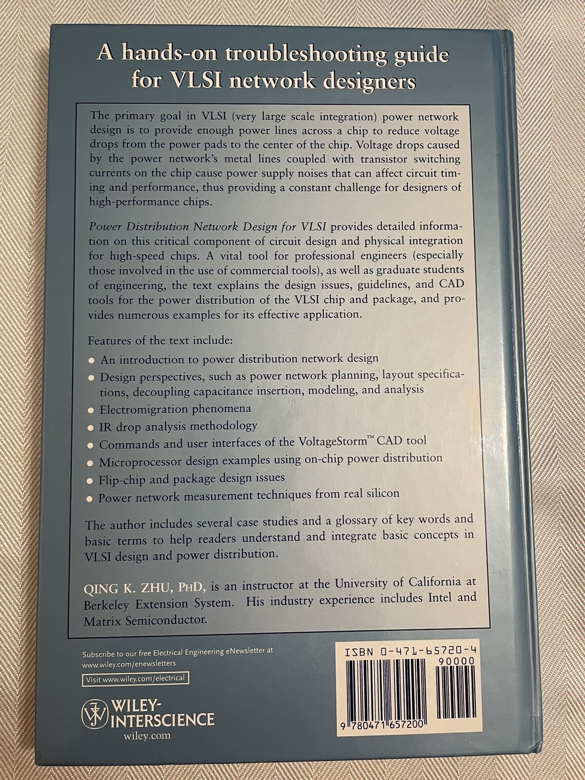
A hands-on troubleshooting guide for VLSI network designers The primary goal in VLSI (very large scale integration) power network design is to provide enough power lines across a chip to reduce voltage drops from the power pads to the center of the chip. Voltage drops caused by the power network s metal lines coupled with transistor switching currents on the chip cause power supply noises that can affect circuit timing and performance, thus providing a constant challenge for designers of high-performance chips. Power Distribution Network Design for VLSI provides detailed information on this critical component of circuit design and physical integration for high-speed chips. A vital tool for professional engineers (especially those involved in the use of commercial tools), as well as graduate students of engineering, the text explains the design issues, guidelines, and CAD tools for the power distribution of the VLSI chip and package, and provides numerous examples for its effective application. Features of the text include: An introduction to power distribution network design Design perspectives, such as power network planning, layout specifications, decoupling capacitance insertion, modeling, and analysis Electromigration phenomena IR drop analysis methodology Commands and user interfaces of the VoltageStorm CAD tool Microprocessor design examples using on-chip power distribution Flip-chip and package design issues Power network measurement techniques from real silicon The author includes several case studies and a glossary of key words and basic terms to help readers understand and integrate basic concepts in VLSI design and power distribution., The common task in a VLSI power network design is to provide enough power lines across a chip to reduce voltage drops. This is a main challenge in high-performance chips as these drops create noise, reducing speed and clarity. This book provides detailed information on the power distribution network design in integrated circuit chips., A hands-on troubleshooting guide for VLSI network designers The primary goal in VLSI (very large scale integration) power network design is to provide enough power lines across a chip to reduce voltage drops from the power pads to the center of the chip. Voltage drops caused by the power network's metal lines coupled with transistor switching currents on the chip cause power supply noises that can affect circuit timing and performance, thus providing a constant challenge for designers of high-performance chips. Power Distribution Network Design for VLSI provides detailed information on this critical component of circuit design and physical integration for high-speed chips. A vital tool for professional engineers (especially those involved in the use of commercial tools), as well as graduate students of engineering, the text explains the design issues, guidelines, and CAD tools for the power distribution of the VLSI chip and package, and provides numerous examples for its effective application. Features of the text include: * An introduction to power distribution network design * Design perspectives, such as power network planning, layout specifications, decoupling capacitance insertion, modeling, and analysis * Electromigration phenomena * IR drop analysis methodology * Commands and user interfaces of the VoltageStorm(TM) CAD tool * Microprocessor design examples using on-chip power distribution * Flip-chip and package design issues * Power network measurement techniques from real silicon The author includes several case studies and a glossary of key words and basic terms to help readers understand and integrate basic concepts in VLSI design and power distribution.
LC Classification Number
TK7874.75Z48 2004
Item description from the seller
About this seller
mjf977
100% positive Feedback•52 items sold
Registered as a private sellerThereby, consumer rights stemming from EU consumer protection law do not apply. eBay buyer protection still applies to most purchases.
Seller Feedback (21)
- r***a (10)- Feedback left by buyer.More than a year agoVerified purchaseExcellent seller! The book's condition was accurately described and it was shipped promptly.Advanced Compiler Design and Implementation by Muchnick, Steven (#125564444047)
- r***i (679)- Feedback left by buyer.More than a year agoVerified purchaseReceived on time, in good condition, and as advertised. Good Seller.Columbia Western-Style Men's M Med Medium Brown Plaid Short Sleeve Shirt (#124789580496)
- n***6 (102)- Feedback left by buyer.More than a year agoVerified purchaseArrived quickly and in condition described.Christianity Among the Arabs in Pre-Islamic Times by J.S. Trimingham - Hardcover (#125647182755)
More to explore:
- Design Non-Fiction Hardcover Books,
- Network Non-Fiction Hardcover Books,
- Networking Non-Fiction Hardcover Books,
- Fashion Design Non-Fiction Hardcover Books,
- Interior Design Non-Fiction Hardcover Books,
- Art & Culture Non-Fiction Fashion Design Hardcover Books in English,
- Art & Culture Fashion Design Non-Fiction Hardcover Books with Dust Jacket,
- Hardcovers Books,
- Web Designer Magazines,
- Hardcover Signed Books